


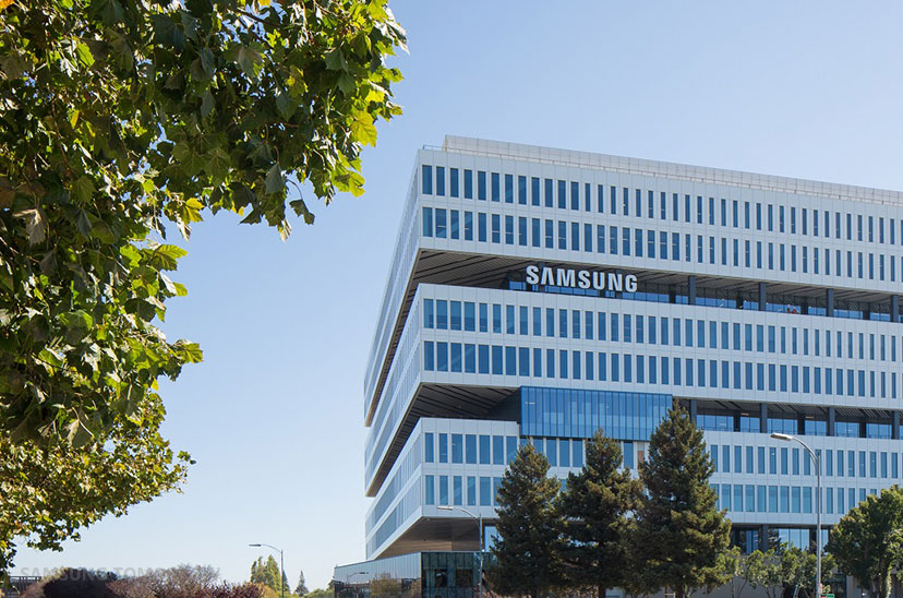
The new Device Solutions America headquarters, 1.1 million square feet in size, is designed as a home to over 700 employees and numerous displays, LEDs, and semiconductor research labs. The new headquarters will also bring together employees in marketing, support, and sales areas, and blend the mingling of employees with in-office gardens (which is said to “increase employees’ contentment and creativity”).
At the company’s announcement of its new semiconductor headquarters, Samsung also took time to create the $1 million STEM College Education Fund for state university students (in California) enrolled in STEM degree programs who can expect one year’s tuition and living expenses from the fund. Samsung also donated $100,000 to the Second Harvest Food Bank and another $100,000 to the Family Giving Tree.
Samsung’s new semiconductor headquarters marks the continuation of the company’s long history of innovation. We’re excited to see Samsung continue to bring “the next big things” to market.