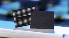
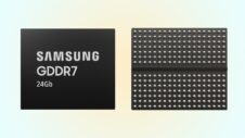
After starting the mass production of 128-layer sixth-generation NAND flash memory chips last year, Samsung had announced the development of 160-layer NAND flash chips two months ago. Now, it is being reported that the South Korean memory chip giant has formed a task force to improve the production yield of its memory chips.
In order to raise its competitiveness in the 128-layer V-NAND chip production, Samsung has set up a task force that includes executives from Samsung Device Solutions' (SDS) Manufacturing Technology Center and from the department that is in charge of the NAND flash production. The new team will solve any issue that arises during chip production and implement steps that improve the productivity of the whole process.
Since Samsung is facing competition from the likes of Intel and YMTC (Yangtze Memory Technologies Co.) in the 128-layer V-NAND memory chip production space, the company wants to make sure that its yield is the highest and its processes are the most efficient in the industry. The company is also investing in expanding the memory chip production capacity.
The South Korean chip giant uses the channel hole etching technology that pierces holes from the top to the bottom of the stacked 128 layers. This provides an electrical connection between layers. The higher the number of layers, the higher the memory capacity. The single stack method indicates a process of piercing holes in one go, and Samsung uses this method in the production of its 6th-generation NAND flash chips for competitive pricing. There's also a double stacking method that involves piercing holes in two steps, but it costs up to 30 percent more.
Piercing holes through a 128-layer NAND flash chip is said to require twice as long when compared to piercing holes through a 96-layer NAND flash chip. Samsung's new task force will try to overcome as many limitations as possible and leave the company's competitors in the dust. This is a part of Samsung's ‘Super Gap' strategy in which the company improves its technology by such a vast margin that it's hard for rivals to catch up.
Samsung has already achieved competitive pricing through its 128-layer NAND flash chip production process, but the company wants to improve even further. By the time Intel and YMTC catch up, the South Korean firm could move to its 160-layer technology, which offers 20 percent higher productivity per wafer. Samsung's semiconductor business has been the saving grace in times when sales of its smartphones and TVs have plunged.


