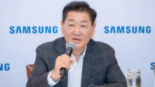
Samsung posted strong financial results for the second quarter of 2020, and the company's flagbearer was its chip business. Amid the COVID-19 pandemic, the demand for memory and storage chips has been rising as more people stay home to learn and work. Now, the company's Vice Chairman Lee Jae-Yong inspected the chip packaging facility in Asan to oversee the future plans.
It is being reported that Samsung heir Lee, who has been visiting the company's various factories and meeting key executives over the past few months, visited the company's Onyang Campus in Asan, South Korea, and checked its future plans in chip packaging solutions. He stressed on preparing the company for the rising demand for advanced semiconductor chips.
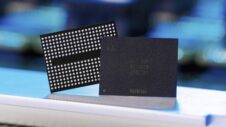
Lee reportedly said, “We must lead the post-pandemic era. We have no time to hesitate.” This is the second time he has visited the facility that specializes in semiconductor packaging. The company said that semiconductor packaging has become a core technology in its business as the demand for high-capacity and low-power chips is rising on the back of strong growth in 5G, AI (Artificial Intelligence), and IoT (Internet of Things) sectors.
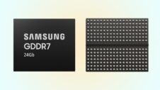
Samsung has been trying to boost its chip packaging technology. In 2018, the company established a test and system package (TSP) division that is dedicated to chip packaging. The South Korean firm is the biggest memory chip maker in the world, and its semiconductor unit brought in $15.2 billion in revenue during Q2 2020, up 13.3% from Q2 2019.
The company had announced earlier this year that it has developed 160-layer 3D V-NAND technology for manufacturing memory chips. It has also set up a task force to improve the yield of its 6th Gen NAND flash chips to make sure that its yield is the highest and its processes are the most efficient in the industry.


