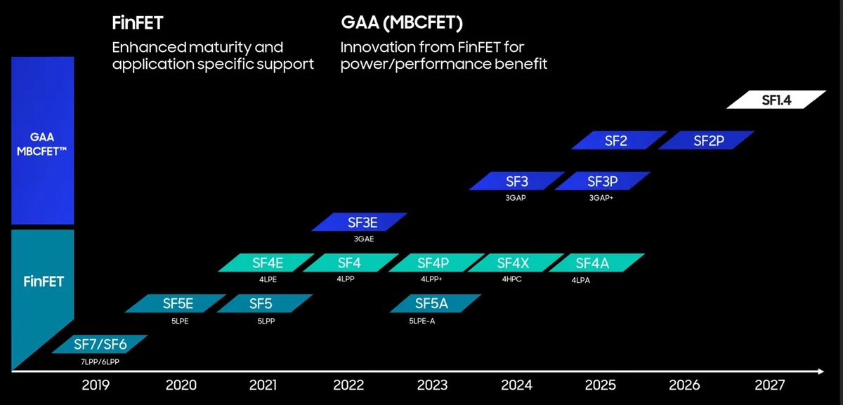
Samsung Foundry, the world's second-biggest semiconductor chip manufacturing firm, announced during the Samsung Foundry Forum 2022 event that it would keep improving semiconductor chips to be smaller, faster, and more power efficient. To that end, the company announced its plans to manufacture 2nm and 1.4nm chips.
Samsung's second and third-generation 3nm GAA chips feature smaller transistor size, better efficiency
But first, let's talk about the company's 3nm chips. Samsung Foundry started the mass production of the world's first 3nm chips (SF3E) featuring GAA (Gate All Around) technology a couple of months ago. GAA is an overhaul of the basic transistor design, which only happens once a few years. The company promises massive improvements in power efficiency with the help of this technology. Samsung is planning to introduce second-generation 3nm semiconductor chips (SF3) by 2024.
The South Korean firm said its second-generation 3nm chips would have 20% smaller transistors than first-generation 3nm chips. This will result in smaller and more power-efficient chips for smartphones, PCs, cloud servers, and wearables.
Samsung plans to further enhance its 3nm transistor fabrication technology with its SF3P+ process and start mass production by 2025. The company has already proved that it can mass produce GAA chips, and its second and third-generation GAA chips could attract some of the big clients it lost (Apple, AMD, Nvidia, and Qualcomm) to TSMC over the past few years.

Samsung Foundry will mass produce 2nm chips in 2025 and 1.4nm chips by 2027
Samsung also announced that it plans to start producing 2nm chips by 2025. This is when the South Korean firm will adopt the backside power delivery for chips. Usually, powering transistors and communicating with them is done only through one side of a semiconductor chip. With the new backside power delivery technology, communication and power delivery are divided into opposite sides of a chip. This improves the overall chip performance. Intel plans to bring a similar feature (PowerVia) to its chips by 2024.
Samsung Foundry also added a new node—1.4nm (SF1.4)—to its semiconductor manufacturing plans. The company plans to start the mass production of 1.4nm chips by 2027. The South Korean firm is yet to reveal what improvements to expect from its 1.4nm chips, but it assures that Moore's Law is still moving, albeit slowly.
The company is also improving 2.5D/3D heterogeneous integration packaging technology. Samsung's 3D packaging X-Cube with micro-bump interconnection will be available in 2024, while bump-less 3D X-Cube will be available in 2026. Samsung also plans to expand chip production capacity by 3x by 2027 compared to 2022.
Samsung is also focusing on automotive and 5G/6G communication markets
The South Korean firm expects 50% of the chip demand to come from automotive, HPC (High-Performance Computing), IoT, and 5G markets. The company will use enhanced 4nm processes to manufacture chips for automotive and HPC segments. It is currently making 28nm eNVM chips for its automotive clients, but it plans to improve that with 14nm eNVM solutions in 2024 and 8nm eNVM solutions in the future.
Samsung is currently making 8nm RF (Radio Frequency) chips for the telecommunications sector and is developing 5nm RF chips that could be launched shortly. The company is also planning “cleanrooms” for its semiconductor factories. These sections will make it easier for the company to store fab equipment and use it later as the demand grows.


