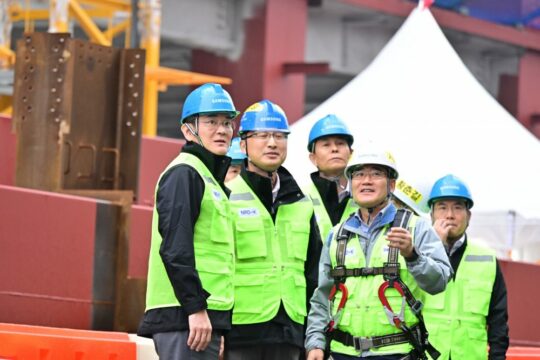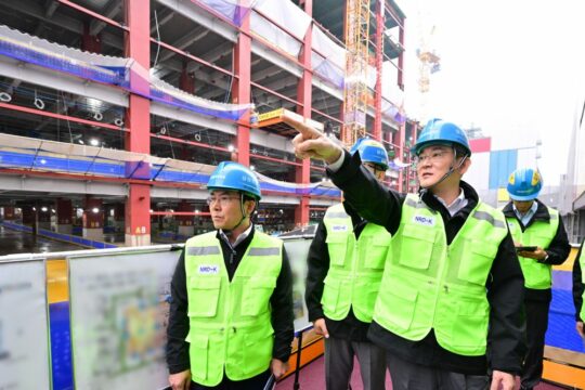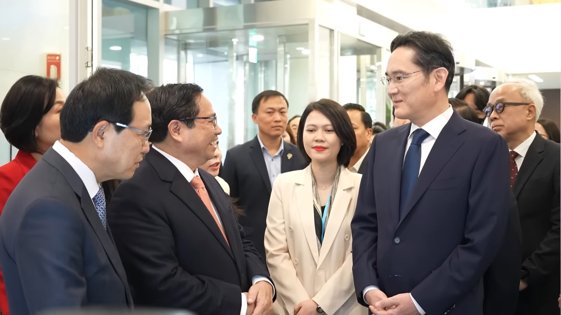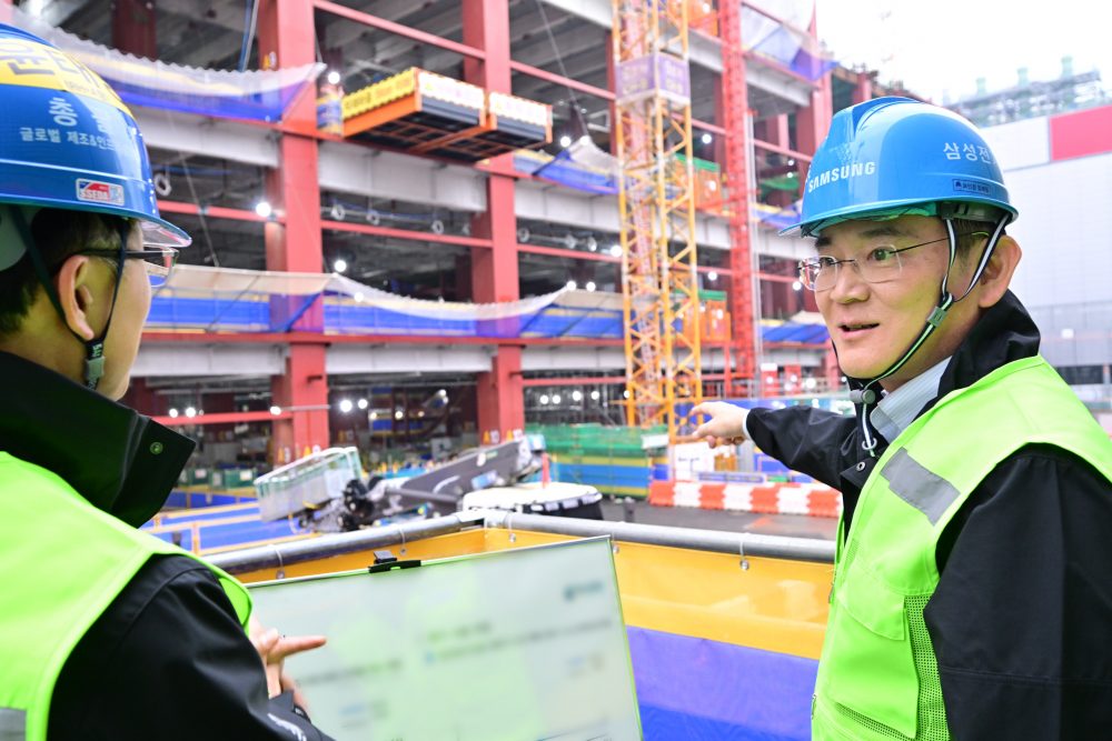
The leader inspected the construction site and held a management meeting with other Samsung executives, some of whom attended through video conferencing as they were overseas.
The management meeting took place at the Samsung Electronics Semiconductor Research Center yesterday. Among the executives who have attended were:
- Kye Hyun Kyung, head of Device Solutions division.
- DS division CTO Jai-hyuk Song.
- Jung-bae Lee, head of Memory division.
- Siyoung Choi, head of Samsung Foundry.
At the private conference, Chairman Lee Jae-yong asked everyone to “provide a turning point for innovation that will enable the semiconductor business to take a leap forward as internal and external crises continue.” The Chairman urged the executives and everyone at Samsung not to waver in times of crisis and underlined the importance of technological leadership.
Story continues after the video
Samsung to invest $15 billion in the new R&D complex
The Korean tech giant announced its plans to construct a new R&D complex for semiconductors last year. Its location: the Giheung Campus in Yongin, Gyeonggi Province.
Despite the recent hurdles faced by the semiconductor market due to economic uncertainties, which led to low demand for chips, Samsung is playing the long-term plan and intends to double the size of the semiconductor research institute “in terms of quality and quantity.”
To achieve this, Samsung plans to invest 20 trillion won ($15 billion) in the new large-scale next-gen R&D complex by 2030. The complex will serve the company's semiconductor research, production, and distribution needs.
Image credit: Samsung
