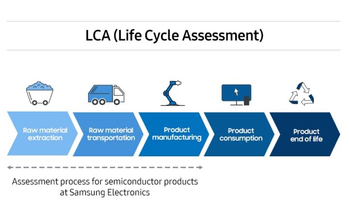
The world leader in semiconductor technology, Samsung Electronics, has recently announced the completion of the Life Cycle Assessment (LCA) on the product carbon footprint for its semiconductors. It has also received certification from DNV, which is one of the world’s leading independent certification bodies.
LCA measures the environmental impacts of commercial products, processes, or services on various parameters such as energy, materials, and waste discharge. Samsung's LCA covers raw materials through chip manufacturing, assembly, and testing, which are in line with ISO 14040, ISO 14044, and ISO 14067.
Since 2019, 37 of Samsung's semiconductor products have received carbon footprint accreditation from the Carbon Trust and UL. Carbon Trust certified 6 Samsung memory products. As per the official blog, Samsung will evaluate the carbon footprints of semiconductors that it manufactures across all of its global manufacturing, testing, and assembly locations in China, South Korea, and the U.S. Moreover, Samsung will expand its LCA to include water and resource footprints to provide a granular assessment and reduce the environmental impact.
JangSup Lee, CEO of DNV Business Assurance Korea, commented on Samsung's recent success: “Together with global business leaders like Samsung, we will continue to take part in creating a more sustainable environment in the future.” By leveraging LCA, Samsung aims to help its customers meet carbon neutrality demands and contribute to environmental sustainability.


