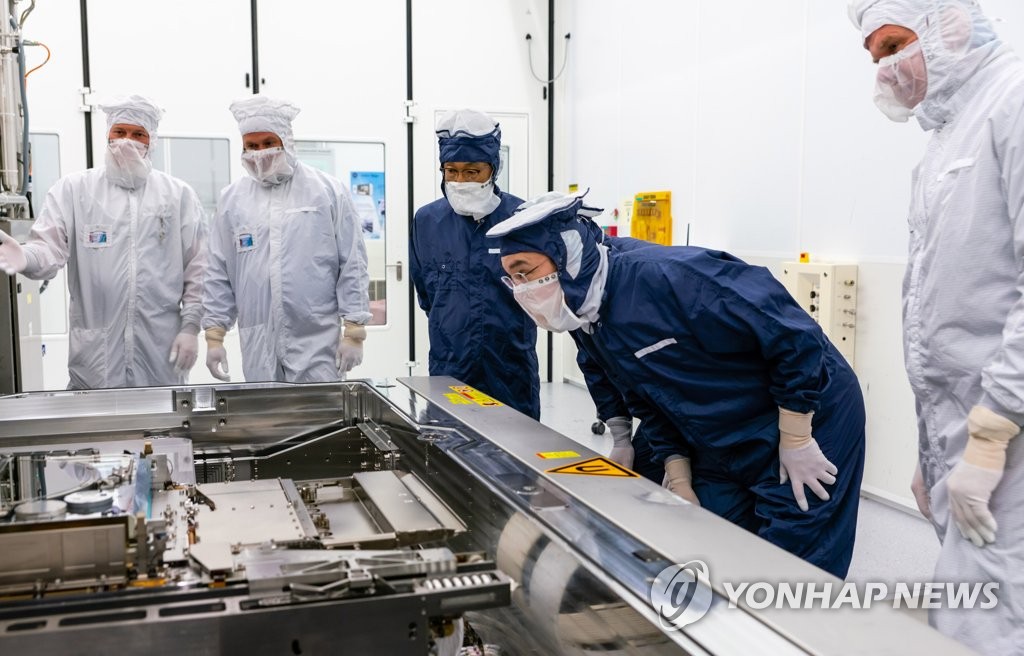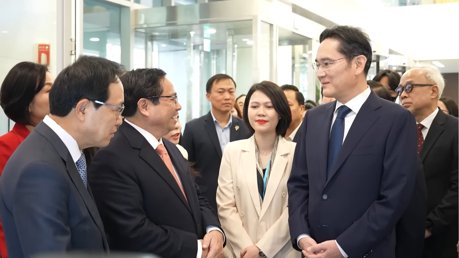
Lee met with ASML's CEO Peter Wennink and CTO Martin Van Den Brink. The meeting was held at ASML's headquarters in Eindhoven in the Netherlands, and the discussions included the supply of equipment necessary for 7nm EUV and lower processes, cooperation on advanced chip manufacturing technology, and the effects of the COVID-19 pandemic on the chip industry. Lee also visited ASML's plant to check EUV equipment.
The South Korean tech giant has been working with ASML since 2000 to improve its chip manufacturing processes. The company even made a strategic investment in ASML in 2012 but sold half of its stake in 2016. Lee had med ASML CEO in South Korean in November 2016 and then in Paris in February 2019. Samsung is trying to boost its competitiveness in the storage and logic chip segments, and trying to catch up with market leader TSMC.
Samsung said in a statement, “EUV lithography is an essential technology to make advanced chips used for artificial intelligence, 5G and autonomous driving applications. Samsung and ASML have been working together to solve technical issues related with EUV technology.”
Recently, Samsung Foundry bagged chip-making contracts from the likes of IBM, Nvidia, and Qualcomm. The company is expected to unveil its first 5nm chipset, the Exynos 1080, for smartphones. However, the Exynos 1080 is not its flagship chipset. The company is expected to unveil the 5nm Exynos 2100 a few weeks before the announcement of the Galaxy S21 series.
