Last updated: July 3rd, 2026 at 09:08 UTC+02:00
SamMobile has affiliate and sponsored partnerships, we may earn a commission.
They could be the most power-efficient chips from Samsung Foundry.
Reading time: 3 minutes
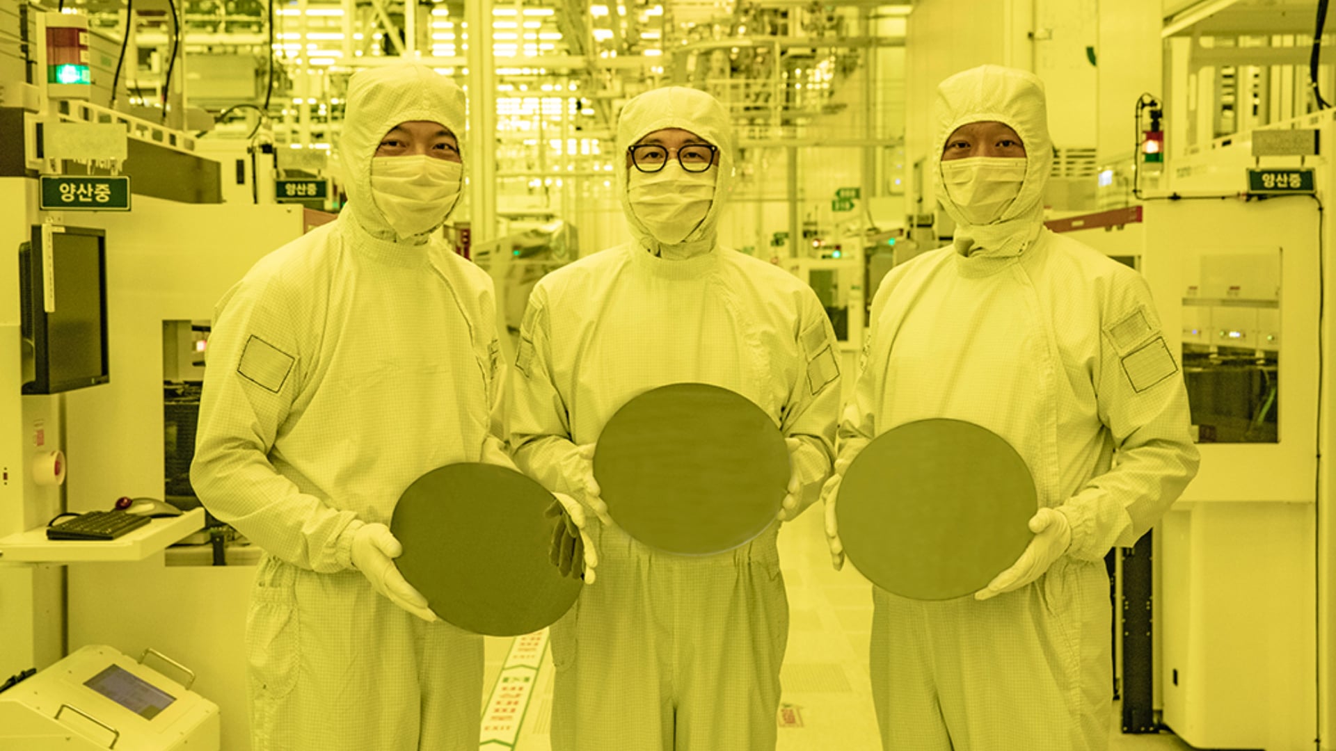
Samsung Foundry
Earlier this week, Samsung revealed more details about its cutting-edge semiconductor fabrication technologies. They include newer-generation 2nm process nodes and its first-generation 1.4nm process. The company has now unveiled its most advanced 2nm process technology, which is scheduled to enter mass production next year.
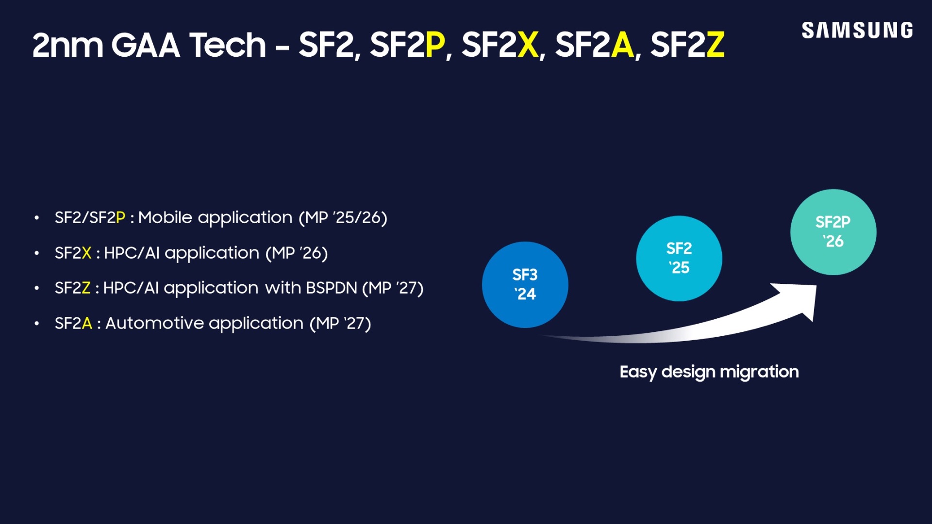
Samsung Foundry is Samsung Electronics’ contract chip manufacturing division. So far, the company has announced six 2nm process nodes:

TrendForce
Samsung Foundry's and TSMC's 2nm process nodes and their roadmaps and timelines compared – Source: TrendForce
Samsung began mass production on its first-generation SF2 process last year. The first chips manufactured using this node are the Exynos 2600 processors used in the Galaxy S26, Galaxy S26+, and the Galaxy Z Flip 8.
Mass production of chips based on the second-generation SF2P process is expected to begin later this year. The Exynos 2700 processor, which is expected to power the Galaxy S27 and Galaxy S27+ in select markets, is rumored to be one of the first chips built on this process. Samsung claims SF2P delivers up to 26% better power efficiency than SF2.
Samsung plans to begin mass production on its third-generation 2nm process, SF2P+, sometime between 2027 and 2028. It is expected to offer further improvements in performance and efficiency over SF2P.
In 2028, Samsung Foundry also plans to begin manufacturing chips using SF2X, a process optimized for AI and high-performance computing (HPC) applications, including AI accelerators used in servers and data centers.
The SF2A process, which Samsung announced in 2024, is missing from the company’s latest roadmap. At the time, Samsung said SF2A was designed for automotive chips used in smart and connected vehicles, with a focus on maintaining reliable operation under extreme temperatures and constant vibration.
Samsung Foundry
Samsung Foundry's 2nm process node roadmap showcased at Samsung Foundry Forum 2024 in the US – Source: Samsung Foundry
During the Samsung Foundry Forum (SFF) 2024 event in the US, Samsung also introduced SF2Z, which features Backside Power Delivery Network (BSPDN) technology.
BSPDN routes the chip’s power lines on the back of the silicon wafer instead of the front. This frees up more space for signal routing, reducing interference while improving performance, power efficiency, and transistor density. However, Samsung didn’t mention SF2Z during its recent SAFE Forum 2026 event, so it remains unclear whether the node has been renamed, merged into SF2P+, or delayed.
Based on the information available today, SF2P+ appears to be Samsung Foundry’s most advanced announced 2nm process for mobile chips, with mass production expected in the second half of 2027 or early 2028. If Samsung follows its usual roadmap, the Exynos 2800 processor could be one of the first chips manufactured using this process.

Asif is a computer engineer turned technology journalist. He has been using Samsung phones since 2004, and his current smartphone is the Galaxy S23 Ultra. He loves headphones, mechanical keyboards, and PC hardware. When not writing about technology, he likes watching crime and science fiction movies and TV shows.