With the 8nm silicon fabrication process, it is possible to create a ‘one-chip solution' for 5G communications that incorporates both multi-channel and multi-antenna design. After 28nm and 14nm RF solutions, the 8nm RF solution will help Samsung in expanding its leadership in the 5G segment on mmWave and sub-6GHz fronts. The company will use this technology to contract manufacture RF 5G chips for other brands.
Digital circuits have seen an increased performance, better area efficiency, and improved power efficiency with each new process node. However, analog and RF blocks haven't seen much success in those aspects due to increased resistance from narrow line width. Hence, most RF chips have seen a degraded performance. To overcome this issue, Samsung claims to have developed a unique architecture using its 8nm process node, and it is called RFextremeFET (RFeFET).
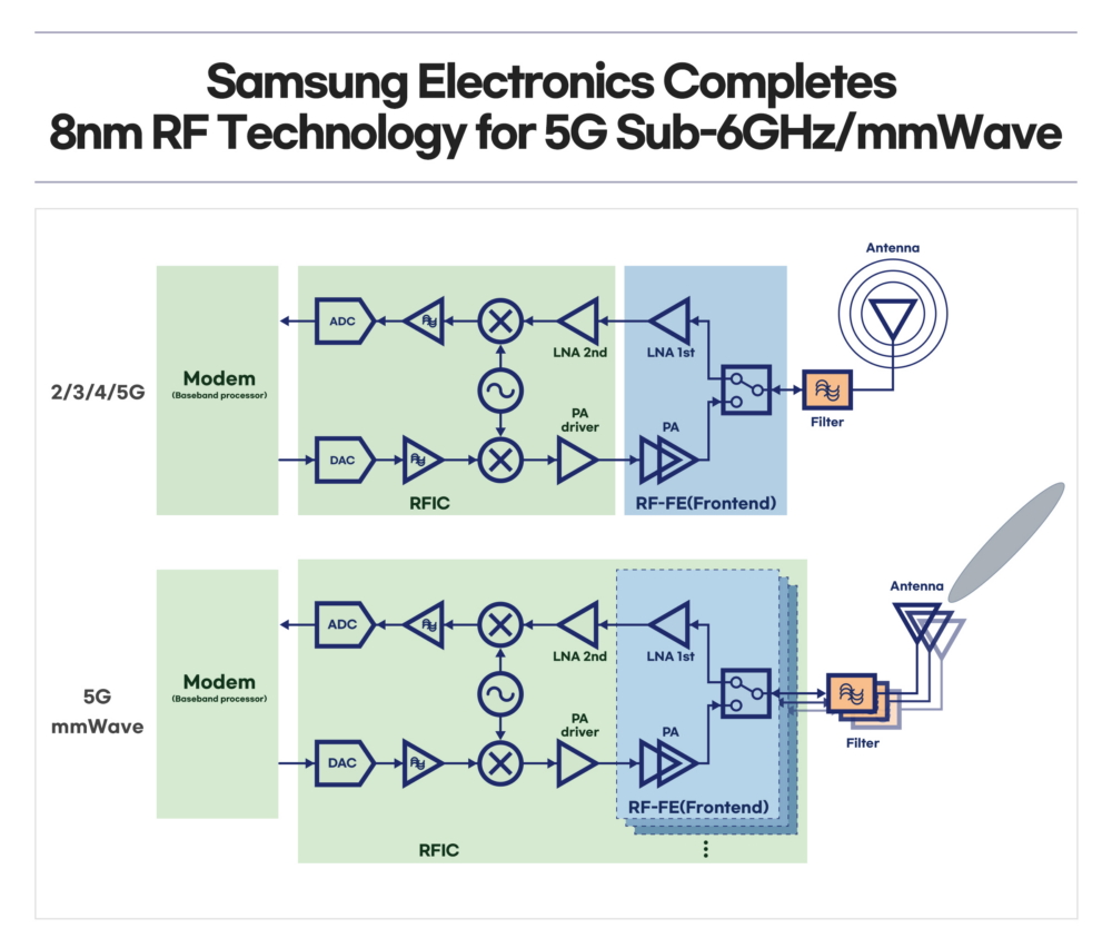
The RFextremeFET architecture offers improved performance and power efficiency. It supplements digital PPA scaling and analog/RF scaling at the same time, which is extremely helpful in enabling high-performance 5G platforms. Samsung Semiconductor claims that its new architecture offers 35% improvement in power efficiency and a 35% smaller die area.
Hyung Jin Lee, Master of Foundry Technology Development Team at Samsung Electronics, said, “Through excellence in innovation and process manufacturing, we’ve reinforced our next-generation wireless communication offerings. As 5G mmWave expands, Samsung’s 8nm RF will be a great solution for customers looking for long battery life and excellent signal quality on compact mobile devices.“
