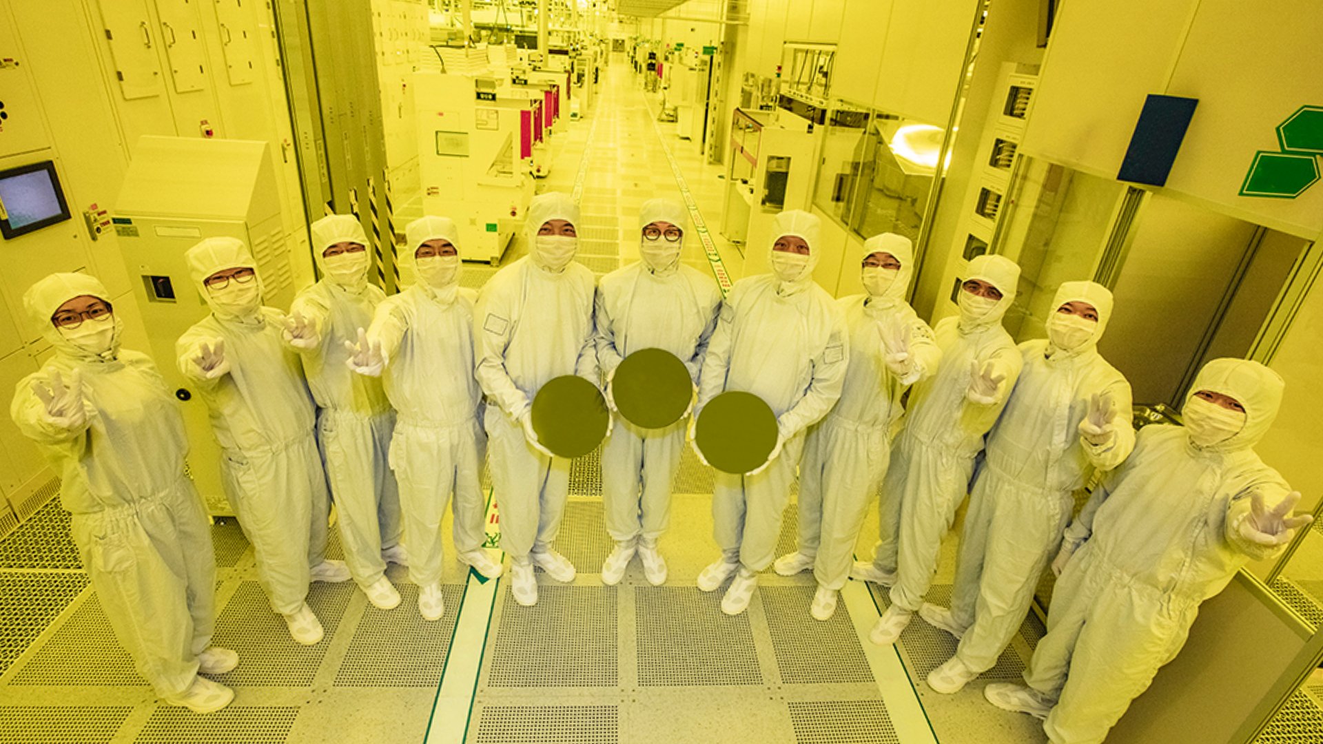
Much has been written about Samsung's troubles with the 3nm process. The yield issue is said to be particularly bad and one of the reasons why the company has been struggling to steal orders away from TSMC. The reported change would signal a shift in Samsung's priorities to focus more on improving crucial aspects of the existing process before jumping to more advanced nodes.
It's time to focus on sorting the 3nm process out
It's claimed that Samsung has dissolved its Foundry Technology Development division that operated under the Semiconductor Research Institute. The research personnel from this division have reportedly been reassigned to other teams within Samsung Foundry that are focused more on yield management, improvement, and process design.
Market watchers interpret this move as a strategy to stabilize Samsung's existing 3nm process as opposed to rushing ahead with the development of advanced nodes below 2nm. The challenges with the 3nm process have become a bit of a reputation issue for the company, and it needs to turn things around if it wants to inspire a lot of confidence in its next-generation nodes.
Only time will tell if this move is too little, too late or better late than never. Samsung Foundry has been bleeding cash recently and the company has been forced to shut production lines to stem the losses. A renewed focus on improving the existing process could go a long way in helping the company recover its momentum that appears to have been loft somewhere in the process of advancing process technology.


