Latest reviews
-
 Samsung Galaxy Watch 8 review
 -
 Samsung Bespoke AI Jet Ultra review
 -
 Samsung Galaxy Z Fold 7 review
 -
 Samsung Galaxy Z Flip 7 review
 -
 Samsung Galaxy S25 Edge review
 -
 Samsung S95F OLED TV review
 -
 Samsung Q7F QLED TV review: A no-brainer purchase at its low price
 -
 Samsung S90F OLED TV review: Unreal value for money
 -
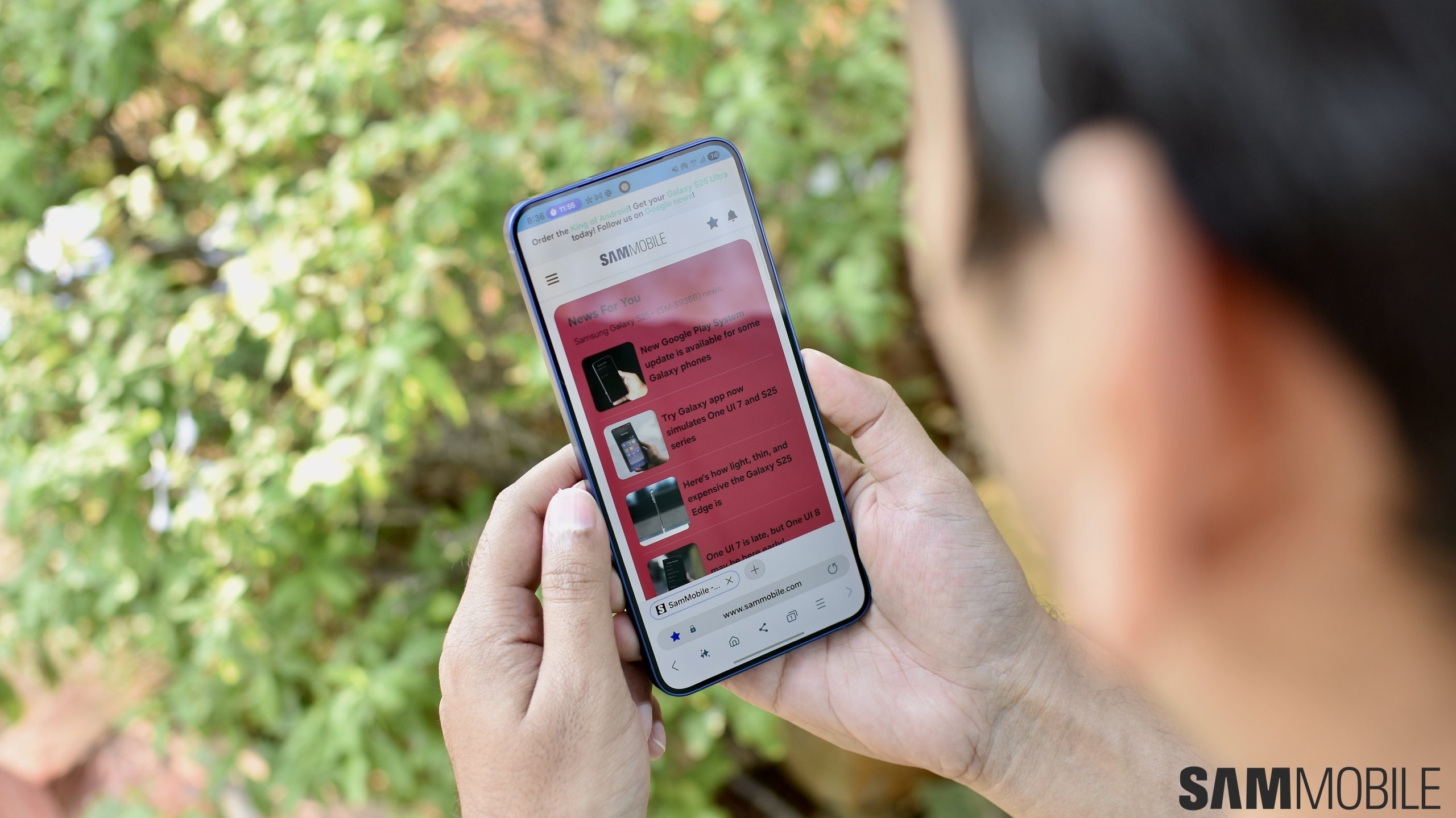 Samsung Galaxy S25+ review: Nails the big phone basics