



Latest opinions
-
 Why I miss when Samsung made weird Galaxy phones
 -
 Apple sets the pace, but Samsung drives the heartbeat
 -
 The two problems Samsung's FE branding causes for both average consumers and fans
 -
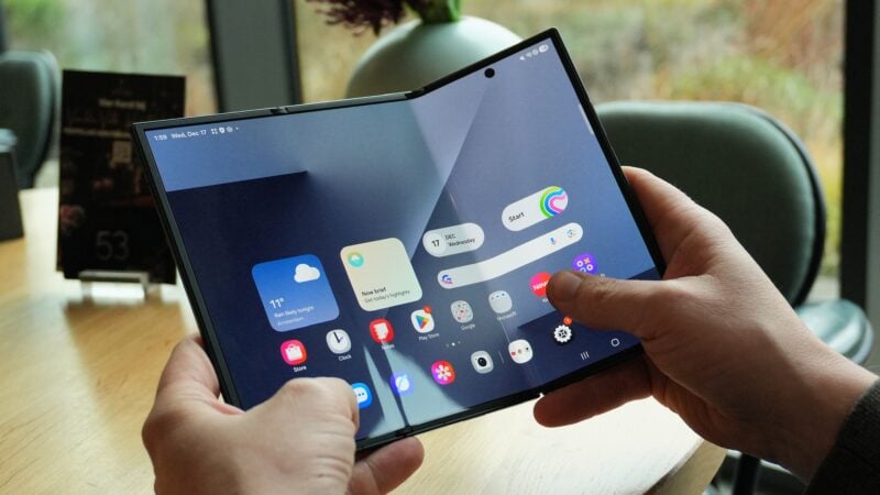
 I love my Galaxy Z Fold 8 so much I worry about ever having to go back
 -
 One of my favorite Galaxy Z Fold 8 features reminds me of old folding clocks
 -
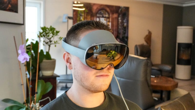
 Samsung's smartglasses promise privacy but won't escape this legal minefield
 -
 Maybe Samsung isn't the problem, maybe bar phone design has simply peaked
 -
 Hot take, but I wish my Galaxy Z Fold 8 had one fewer selfie camera
 -
 Samsung wants iPhone users to feel at home on Galaxy



